- Daily Market Exchange Newsletter
- Posts
- TSMC's Data Flywheel: The Real Barrier to Intel's Comeback
TSMC's Data Flywheel: The Real Barrier to Intel's Comeback
TL/DR: $TSM remains the only bankable choice for volume production of the most advanced chips today.
TSMC's Data Flywheel: The Real Barrier to Intel's Comeback
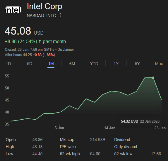
The 2026 narrative for $INTC is seductive: Western hyperscalers, under intense pressure to derisk from the Taiwan Strait, are handing $INTC a golden ticket.
However, Intel’s earnings call last week served as a reality check: not all fabs are created equal. Intel and TSMC may use the same ASML machines, but having the same oven doesn’t mean you can bake the same cake.
To understand Intel’s uphill battle, you have to look at the "invisible" physics of chipmaking.
1.The Yield Loop: Why TSMC is a Data Monopoly
$TSM didn't win by accident; they built a self-reinforcing flywheel.
Buying Data: From Day 1, TSMC priced wafers low to secure massive volume. This wasn't just for revenue—it was to harvest fault data.
More wafers = more lessons: Because TSMC ran 10x more wafers than anyone else, they could iterate 10x faster. They identify a defect, tweak the "recipe," and redeploy. By the time a competitor even starts their production run, TSMC has already moved up the learning curve, perfecting its yield "recipe."
Cost Leadership: Higher yields = more usable chips per wafer. This gives TSMC significant cost advantages and the ability to maintain profitability even at competitive prices.
Reinvestment and Expansion: Profits from each cycle were reinvested into expanding fab capacity ($30B+ annual CapEx), further solidifying volume dominance and perpetuating the self-reinforcing moat.
2. Chipmaking Isn't "Cookie-Cutter"
A common misconception is that if you buy a $400M ASML machine, you automatically get 2nm chips. In reality, the machine is just the "oven." The yield is the "recipe," and that recipe is a closely guarded trade secret.
The Recipe Variable: A single chip goes through 1,000+ steps. A 1-degree temperature variance in a chemical vapor deposition (CVD) chamber or a 0.5-second difference in a plasma etch can tank a wafer's yield.
Human Capital & "Tribal Knowledge": Yield improvement is a forensic science. It requires an army of engineers who can look at a microscopic defect and know exactly which of the 1,000 steps caused it. TSMC has decades of this specialized "muscle memory."
3. Intel’s "Equalizer" Moment
We are currently at a rare reset in chip architecture. The shift from FinFET to Gate-All-Around (GAA) transistors forces everyone, including TSMC, onto a new learning curve.
Intel’s 18A Leapfrog: Intel is betting on PowerVia (Backside Power Delivery, “BSPD”). By moving the "power plumbing" to the back of the chip, they’ve hit a 2026 performance milestone that TSMC won't match until their A16 node late this year/early 2027.
But will that be enough?
4. TSMC’s Customer Lock-In
The "Neutral" Model: Unlike Intel or Samsung, TSMC doesn’t design its own chips, so $NVDA, etc. never have to worry about their manufacturer becoming a competitor.
Packaging Lock-in: TSMC’s CoWoS (Chip-on-Wafer-on-Substrate) packaging is the industry standard for AI GPUs. Controlling both the chip and the "envelope" creates a massive lock-in effect.
The Porting Nightmare: Each foundry has a unique Process Design Kit (PDK)—the "rulebook" for how transistors are shaped. Engineers must manually redraw and re-verify millions of circuit paths to match Intel’s specific 18A physical dimensions and electrical properties. Moving a complex AI chip from TSMC to Intel would take 6 to 18 months and tens of millions in requalification costs.
Scale Economies: Because TSMC manufacture for everyone (Apple, Nvidia, AMD), they can afford the staggering CapEx required for new nodes. A competitor cannot match TSMC’s unit cost without matching their massive volume, which creates a "Catch-22" for rivals like Intel.
5. Market Realities
Intel's 18A (1.8nm-equivalent) may lead in raw performance/power, but TSMC's N2 offers higher transistor density and better SRAM scaling; and TSMC's A16 (1.6nm) is introducing BSPD by late 2026/early 2027.
Today, TSMC's N2 yields at ~70-80%, ahead of Intel's 18A at ~60% and Samsung's SF2 at ~40-50%; this reinforces TSMC's edge in volume production reliability, critical for high-stakes chip launches.
"Buy American" tailwinds and gov subsidies are pushing $INTC hype.
Yet, $TSM remains as the only bankable choice for volume production of the most advanced chips today.
Intel's catch-up? A multi-year slog.
For more trade ideas visit the Daily Market Exchange.
Subscribe to receive more Trade Alerts.
About Us
The Daily Market Exchange is a global community where passionate investors and traders share ideas, strategies, and market insights. Stock selection is challenging, and market timing is even tougher—why tackle them alone?
Our members benefit from the collective wisdom and experience of a global network. Unsure about a stock idea? Collaborate with others to refine your research and gain confidence from their sector expertise. Struggling to find fresh trade ideas? Join the Daily Market Exchange today and access our members’ latest analysis and market strategies!
Read more about us HERE.

Disclaimer: The information provided here is for informational and educational purposes only and should not be considered financial, investment, tax, or legal advice. All opinions, analyses, and suggestions are based on publicly available data and general observations, not personalized recommendations. Stock prices, market conditions, and financial outcomes can change rapidly—always verify data independently. Past performance is not indicative of future results, and investing involves risk, including the potential loss of principal.